Chuck Marks in Sol-Gel Coatings Dunbar P. Birnie, III
After noticing puzzling color variations (indicating thickness difference
patterns) in sol-gel coatings that we had been depositing on glass (to
make multilayer interference filters and other
devices) --- see photo at right + click to enlarge --- we (myself, in collaboration
with Prof. Zelinski and with the help of Dr. Melpolder of Kodak)
designed experiments to reach a better understanding of how these thickness
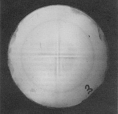
patterns formed during the spin-coating process.The figure at left just
below shows some subtle patterning in coating appearance that formed on
a glass wafer, where the pattern of back-side-contact with the vacuum chuck
matches the pattern shown. All areas were transparent, but showed rather
subtle reflectance appearances. Ellipsometry measurements determined that
the darker areas were physically thicker than the lighter areas in this
picture. The darker (thicker) areas corresponded with areas that had good
physical contact with some material in the vacuum chuck. Areas that were
above vacuum grooves or were prevented from making physical contact (e.g.
by hanging out over chuck edge) were thinner.
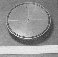
For comparison,
the figure at the right (slightly different magnification) shows the appearance
of the vacuum chuck that was used when making the coating shown above (the
ruler is in inches). The vertical and horizontal lines are tiny grooves
machined in the flat metal surface; the o-ring protrudes slightly above
the level of the metal mesa, thus preventing good wafer/chuck contact in
the outer region (other than where the o-ring touches the wafer), so the
cross-shaped chuck mark feature is mostly evident near the center of the
wafer.
The most unusual
part of these thickness variations is that there was never physical contact
on the top side of the substrate, only contact on the back side using the
vacuum chuck of the spin coater. Thus, there must be some form of "communication"
between the metal in contact on the back side and the coating solution
on the top side.
Our experiments
tested the effect of substrate type (glass, silicon, and thin polymer)
on coating uniformity, especially in patterns related to the vacuum grooves
in the chuck holding the wafers in place during spinning. In addition,
we tested spin duration, solution temperature, and firing temperature. This
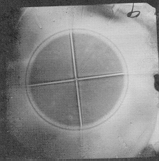
figure shows the chuck mark created when coating the very thin plastic
substrate. This material was much thinner than the glass sample shown above,
so it was able to flex down and form better contact with more of the metal
vacuum chuck parts. One assumes that the areas above the vacuum grooves
was also bowing down somewhat as well. Interestingly, these areas over
the vacuum lines were still the thinnest parts of coating on this sample
(i.e. fluid was not simply being collected in the low spots --- on the
contrary in fact!). Because the much thinner substrate allowed better thermal
conductivity "communication" between the coating solution and the vacuum
chuck, then the chuck mark was printed with much higher detail -- presumably
because local temperature differences were more pronounced.
In general,
we found that coatings that were on substrate areas that had their back
side in direct contact with the metal of the vacuum chuck were systematically
thicker than regions over vacuum grooves. We also noted some differential
edge effects where corners and edges of these metal regions had even thicker
coatings. These two observations were suggested to be attributed to solvent
evaporation effects. Our final explanation was that solvent evaporation
was producing noticable cooling of the solution and wafer top-side and
that this surface cooling was being counter-balanced by heat flow effects
from the metal vacuum wafer holder. And, rather minute temperature differences
from place to place across the substrate surface were impacting the thickness
of coating formed from our sol-gel solutions. In other words:
(1) areas without
metal contact were more significantly affected by the evaporative cooling
effect,
(2) the lower
temperature in these areas caused a lower evaporation rate there too, and
(3) this lower
evaporation rate translated into lower end-point coating thicknesses.
This explanation is completely compatible with Meyerhofer's
seminal model that explained the connection between solvent volatility
and final coating thickness.
The above findings are described in more detail in:
D. P. Birnie, III, B. J. J. Zelinski, S. P. Marvel, S.
M. Melpolder, and R. Roncone, "Film/Substrate/Vacuum-Chuck Interactions
During Spin Coating", Optical Engineering, 31, 2012-2020 (1992).
(c) 1998, Dunbar
P. Birnie, III
Department of Materials Science and Engineering
Rutgers, The State University of New Jersey
 After noticing puzzling color variations (indicating thickness difference
patterns) in sol-gel coatings that we had been depositing on glass (to
make multilayer interference filters and other
devices) --- see photo at right + click to enlarge --- we (myself, in collaboration
with Prof. Zelinski and with the help of Dr. Melpolder of Kodak)
designed experiments to reach a better understanding of how these thickness
patterns formed during the spin-coating process.The figure at left just
below shows some subtle patterning in coating appearance that formed on
a glass wafer, where the pattern of back-side-contact with the vacuum chuck
matches the pattern shown. All areas were transparent, but showed rather
subtle reflectance appearances. Ellipsometry measurements determined that
the darker areas were physically thicker than the lighter areas in this
picture. The darker (thicker) areas corresponded with areas that had good
physical contact with some material in the vacuum chuck. Areas that were
above vacuum grooves or were prevented from making physical contact (e.g.
by hanging out over chuck edge) were thinner.
After noticing puzzling color variations (indicating thickness difference
patterns) in sol-gel coatings that we had been depositing on glass (to
make multilayer interference filters and other
devices) --- see photo at right + click to enlarge --- we (myself, in collaboration
with Prof. Zelinski and with the help of Dr. Melpolder of Kodak)
designed experiments to reach a better understanding of how these thickness
patterns formed during the spin-coating process.The figure at left just
below shows some subtle patterning in coating appearance that formed on
a glass wafer, where the pattern of back-side-contact with the vacuum chuck
matches the pattern shown. All areas were transparent, but showed rather
subtle reflectance appearances. Ellipsometry measurements determined that
the darker areas were physically thicker than the lighter areas in this
picture. The darker (thicker) areas corresponded with areas that had good
physical contact with some material in the vacuum chuck. Areas that were
above vacuum grooves or were prevented from making physical contact (e.g.
by hanging out over chuck edge) were thinner.
 This
figure shows the chuck mark created when coating the very thin plastic
substrate. This material was much thinner than the glass sample shown above,
so it was able to flex down and form better contact with more of the metal
vacuum chuck parts. One assumes that the areas above the vacuum grooves
was also bowing down somewhat as well. Interestingly, these areas over
the vacuum lines were still the thinnest parts of coating on this sample
(i.e. fluid was not simply being collected in the low spots --- on the
contrary in fact!). Because the much thinner substrate allowed better thermal
conductivity "communication" between the coating solution and the vacuum
chuck, then the chuck mark was printed with much higher detail -- presumably
because local temperature differences were more pronounced.
This
figure shows the chuck mark created when coating the very thin plastic
substrate. This material was much thinner than the glass sample shown above,
so it was able to flex down and form better contact with more of the metal
vacuum chuck parts. One assumes that the areas above the vacuum grooves
was also bowing down somewhat as well. Interestingly, these areas over
the vacuum lines were still the thinnest parts of coating on this sample
(i.e. fluid was not simply being collected in the low spots --- on the
contrary in fact!). Because the much thinner substrate allowed better thermal
conductivity "communication" between the coating solution and the vacuum
chuck, then the chuck mark was printed with much higher detail -- presumably
because local temperature differences were more pronounced.